詢價車
關於我們
鈦昇美國
鈦昇介紹
有關鈦昇
發展沿革
鈦昇願景
核心技術
全球據點
鈦昇組織
安全規範
投資人資訊與市場訊息發展
利害關係人
聯絡我們
技術服務
TGV workshop
Laser process development
Small scale production
科技技術能力
Advanced Packaging (AP)
Fan Out PLP
Plasma treatment
EMC residue removal
Copper oxide removal
PECVD
Plasma healing
Plasma dicing
Laser micromachining, Silicon
Thin wafer dicing
Wafer grooving
Laser micromachining, Glass
TGV, through glass via
Glass cavity/frame
Glass cutting
Laser micromachining, Wafer Level Package
Hybrid laser & plasma drilling
Fan-in wafer dicing
SiC Solution
Wafer dicing
Plasma cleaning
Laser ID Marking
Backend Process Solution
產品介紹
雷射解決方案
雷射打印
Wafer
WID 系列
WB 系列
Package
L/F – Substrate - Boat
LM 系列
Blazon 系列
Tray
Laser On Tray 系列
Others
雷射加工
Wafer & Frame Form
WBS系列
WD 系列
WS 系列
GC 系列
L/F – Substrate
Others
高階檢測儀器
電漿技術科技
Plasma Dicing
Wafer Form
Panel Form
L/F – Substrate – Others
腔體式
In-line式
實驗室檢測儀器
UniDRON
FPC 設備
RTR
STS
壓合機
成型機
銅電鍍線
開蓋機 用於軟硬複合板
載帶包材
投資人專區
公開資訊觀測站
企業ESG專區
企業永續發展
氣候變遷風險調適
內部碳定價政策
發展永續環境
環境監測申報報告書
各項預防計畫
溫室氣體盤查
環境管理制度與執行情形
企業永續報告書
供應商管理政策
客戶權益維護與申訴管道
利害關係人溝通管道
員工福利措施、退休制度與其實施情形
企業社會責任實施成效
資訊安全管理政策與執行情形
股東專區
股東會相關訊息
法人說明會資料
財務專區
財務報告書
企業年報
公司治理
公司基本資料
公司治理架構
組織運作規章
董事會資訊
薪資報酬委員會運作情形
審計委員會運作情形
董事會及功能性委員會績效評估
獨立董事與內部稽核主管及會計師溝通政策
誠信經營
防範內線交易
內部稽核
投資人關係聯絡窗口
利害關係人專區
新聞專區
重大訊息公告
展覽活動
粉絲團活動
繁
En
简
繁
|
En
|
简
詢價車
(
)
聯絡我們
首頁
關於鈦昇
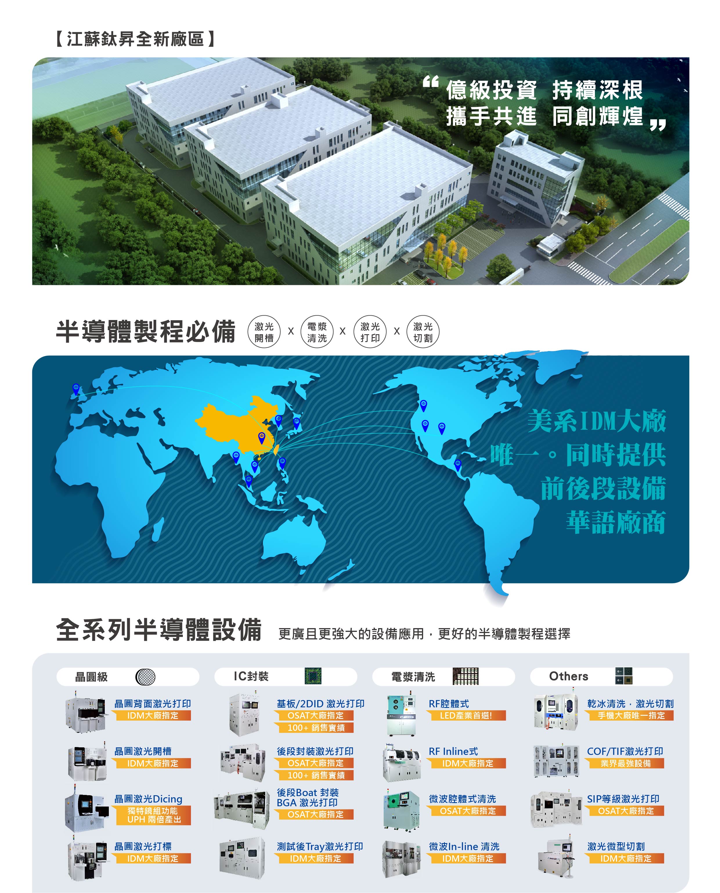
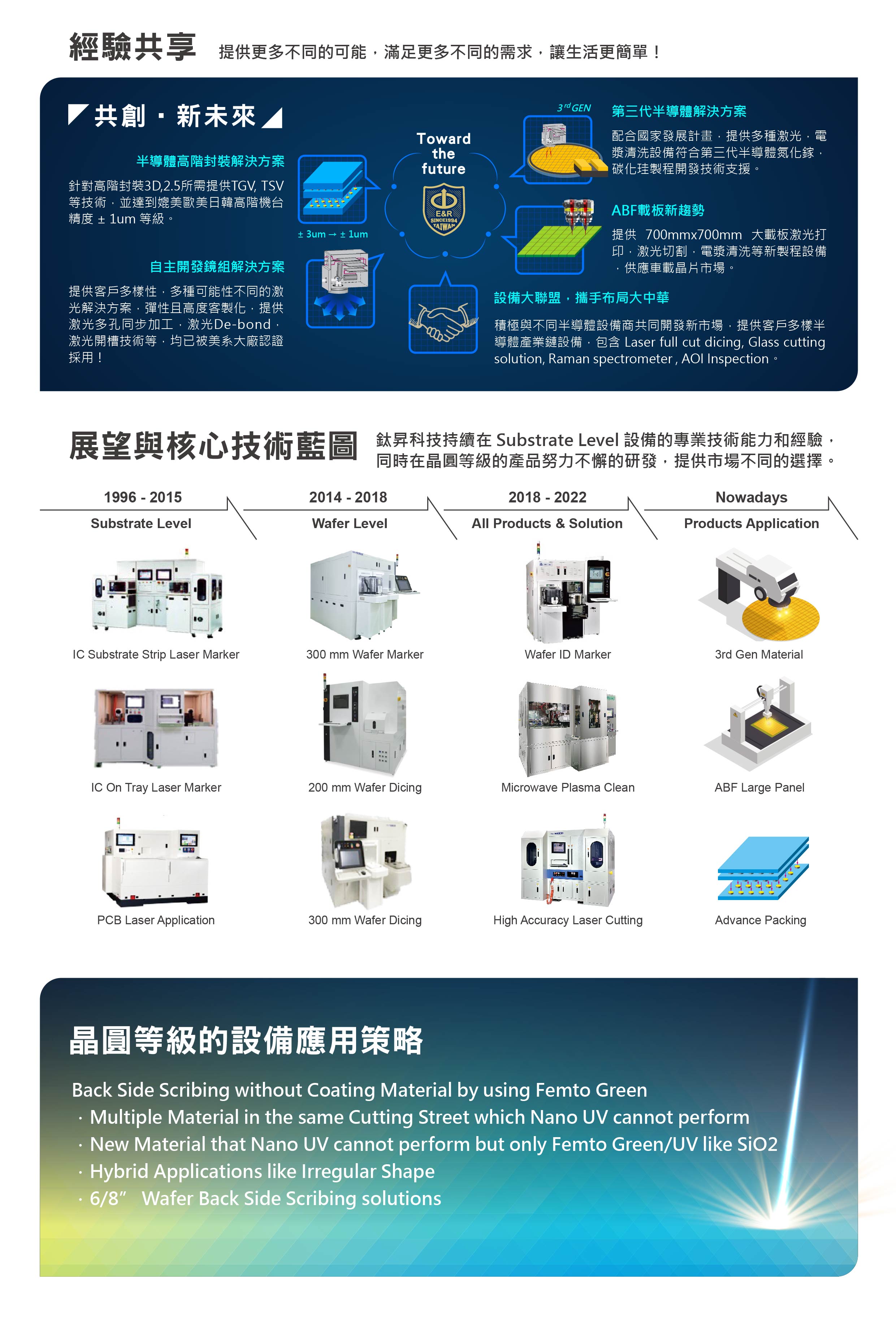
鈦昇科技未來展望技術藍圖
鈦昇科技未來展望技術藍圖