Plasma dicing
Once chips on the wafer become smaller & thinner, traditional dicing technique, e.g. blade saw, faces many challenges, including high-percentage material loss resulted from the width of the dicing street, mechanical damage such as chipping, and unacceptable processing time.
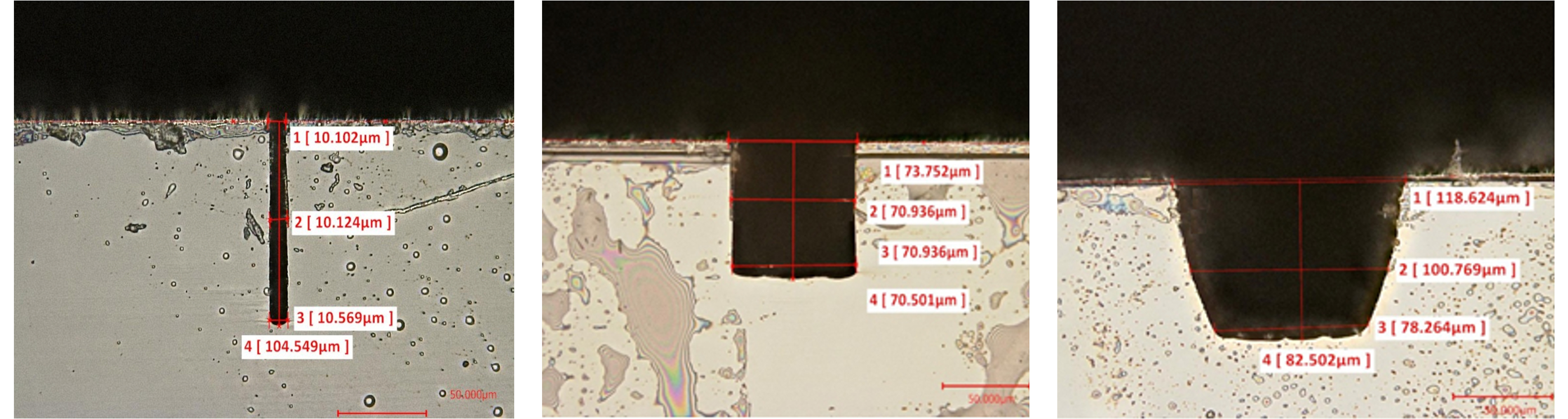
Plasma dicing is a process which uses a dry etching, where all the dicing lanes on the same wafer are cut simultaneously, without die stressing, no contamination, and several-folds in wafer dicing throughput. Also, more chips can be designed onto the wafer as narrower dicing lanes can be employed.
E&R’s plasma dicing system apply unique Microwave etching technology to generate following advantages.
● Low temperature process, no risk to damage the dicing tape.
● No ESD damage in light of downstream plasma
● Non-scallop process, without stress concentration
● Applicable for non-rectangular dicing
● Multiple smaller wafers in-parallel processing
● Low Cost-of-Ownership