
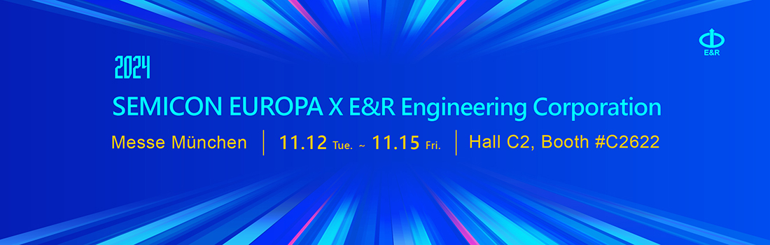
※〔展覽快訊〕2024 SEMICON EUROPA 慕尼黑半導體展 11/12-11/15 In Munich
Glass Substrate Solutions
Glass is emerging as a critical material for next-generation semiconductor technology, especially as a potential interposer material to replace silicon. Its low warpage and high heat resistance make it ideal for integrating more transistors, which is essential to meet the demands of AI and high-speed computing. As the leader in TGV (Through Glass Via) solutions—the foundational step in glass core fabrication-E&R provides a high-throughput TGV solution with a VPS (via per second) reaching up to 8,000 in matrix and 600-1,000 for random patterns, achieving ±5μm accuracy. We also accommodate large glass panels up to 515 x 510 mm, with thicknesses ranging from 0.2 to 1.1 mm.
FOPLP (Fan-Out Panel Level Packaging)
E&R offers reliable, mass-production equipment for FOPLP processes, supporting panel sizes from 300 x 300 mm to 700 x 700 mm. Our solutions include laser marking, laser cutting, plasma cleaning post-drilling, de-smear, laser debonding, post-debond plasma descum, and ABF drilling, all with excellent warpage handling capabilities of up to 16 mm, ensuring high-efficiency output.Plasma Dicing – Small Die Dicing
Our hybrid solution combines laser grooving and plasma dicing, with precise control of cutting channels between 10 μm and 30 μm. Beyond equipment manufacturing, E&R also provides an all-in-one small die dicing service, capable of processing wafers into small dies of various shapes, including hexagons, circles, and MPR shapes, to meet diverse customer requirements.Next generation material: Silicon Carbide (SiC)
Silicon Carbide (SiC) is a key material in the semiconductor industry, particularly as high-power ICs are in demand in the EV and 5G markets. However, challenges arise during backside electrode fabrication. E&R’s advanced technology suite, featuring laser direct cutting, plasma etching for defect removal, plasma de-carbonization, PIII, laser annealing, and PVD solutions, supports customers in manufacturing devices with high-temperature resilience, superior voltage tolerance, and minimal power loss. Additionally, our fully automated Raman inspection system enhances doping quality and stress measurement, reducing yield loss and driving greater economic value.Global Service
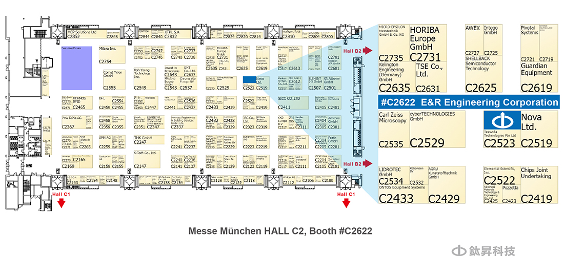
E&R’s primary strengths are our flexibility, expertise in meeting customized requirements, and robust service support. With over 10 service bases and a strong human resource network across Taiwan, China, Southeast Asia, the US, and Europe, we offer extensive global reach. Supported by more than 50 Field Service Engineers worldwide, we provide rapid response to issues and continuous process improvement for our clients.You are cordially invited to visit E&R at MESSE MÜNCHEN Hall C2 Booth #C2622, to explore the latest trends in advanced packaging process technology.
2024-11-01